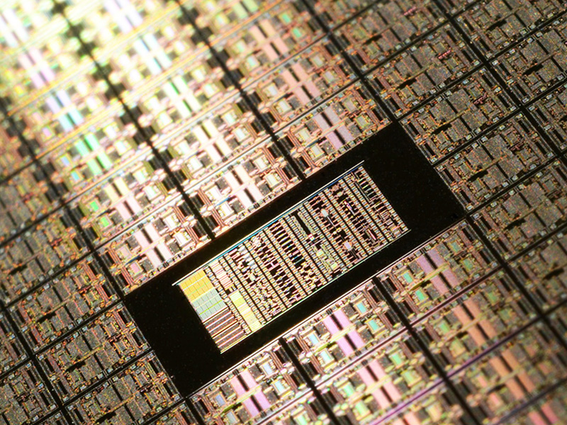
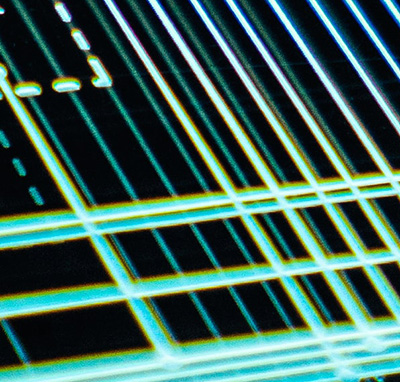
Photolithography is a key process in the manufacturing of semiconductors.
The process begins with a photomask of electronic circuits. This photomask is essentially a template for the chips that will be produced on the silicon wafer. UV or EUV light is then shown through the mask and a series of lenses onto the wafer, resulting in the patterning of the silicon. This process is repeated until the silicon is completely patterned on all layers. The patterned wafer can then enter the next step of production. This patterning of the silicon by the process of photolithography is a vital step in the very delicate and tedious process of wafer chip production.
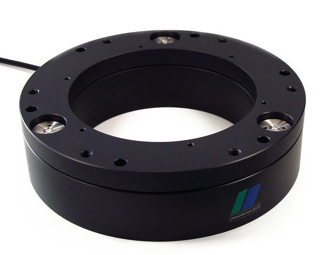
The semiconductor lithography process is extremely precise and typically includes piezo positioning components.
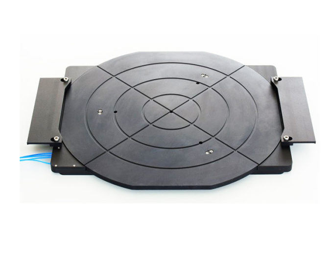
As with every step of semiconductor manufacturing, the positioning of the wafer during photolithography is extremely important. If the wafer is out of position, the silicon will not be patterned correctly. For this reason, piezoelectric stages are commonly used to position the wafers during this step of production. Providing up to 5 axes of motion with nanometer and microradian precision, piezo stages provide a perfect solution for this highly technical procedure.
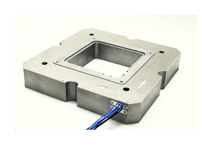
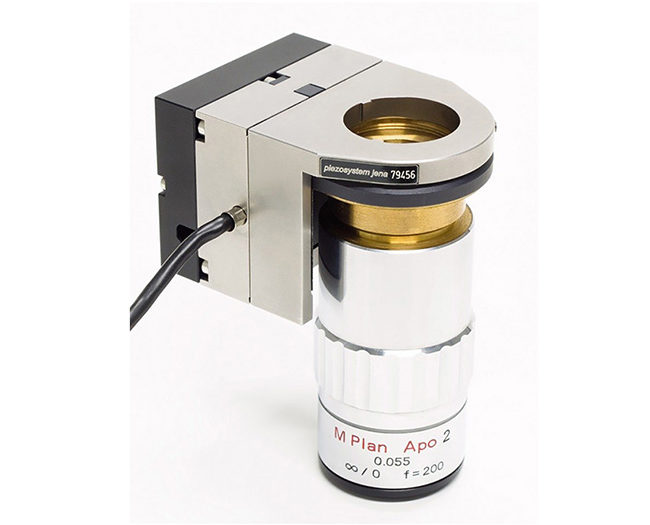
Equally important during the photolithography process is the positioning of the lenses/objectives as they are responsible for focusing the light on the wafer. piezosystem jena has stages and microscope objective positioners (MIPOS) to aid in exactly this task.
Whitepaper: Beyond Microscopy – MIPOS in Industry Applications