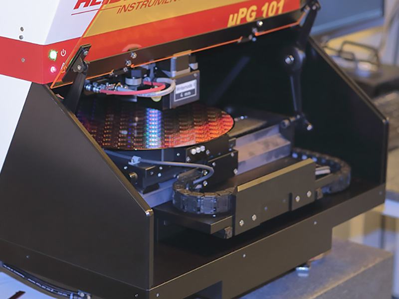
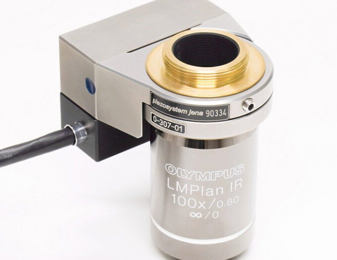
During the semiconductor wafer lithography, inspection, and dicing processes, the exact positioning of the wafer is critical. Today’s roadmap consists of features down to single digit nanometers, meaning the positioning system needed to create these features must have even smaller resolutions. Piezo actuators serve as the perfect tools to create this extremely precise and accurate positioning.
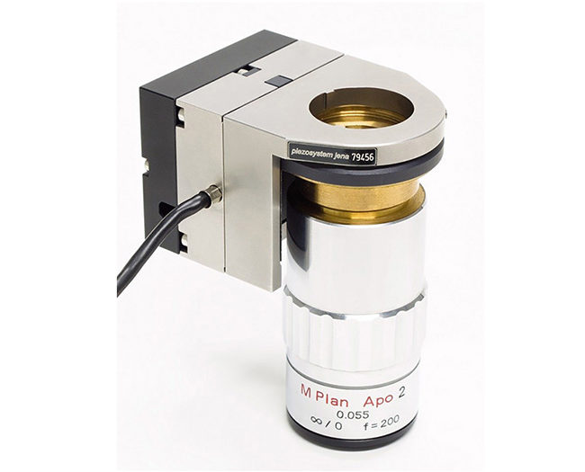
Piezo actuators are used as an OEM component in a variety of semiconductor production machines. Piezo stages move the wafer on demand in sub-nanometer steps per alignment marks or manual adjustment by an operator.
Piezo Solutions for Semiconductor Manufacturing Applications
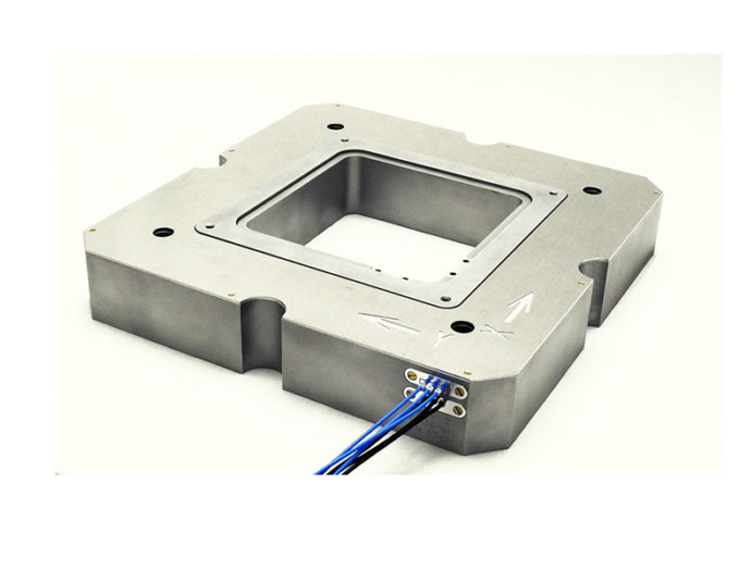
Piezo stages from piezosystem jena utilize a FEM optimized flex hinge design to ensure the highest performance during this wafer positioning process. The benefits include:
- The solid-state design allows for no mechanical wear, ensuring a long and consistent lifetime for the piezo.
- The stages are optimized for high straightness to prevent undesired translational movement.
- Stages can be used in vacuum or UHV environments, which is necessary in the wafer production process.
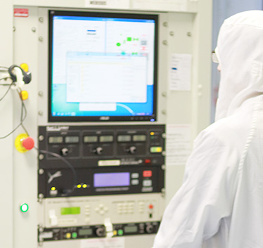
Software, controllers and wafer positioners work together to carefully align wafers for testing, inspection and cutting.
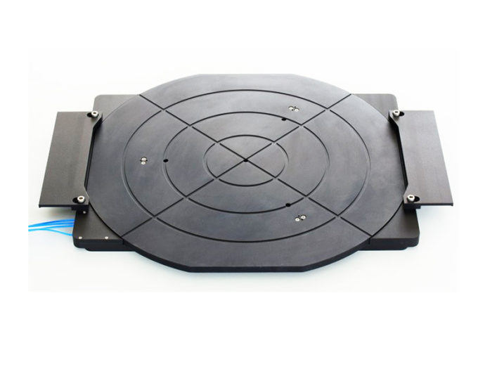
In addition to a wide range of commercial off-the-shelf stages, piezosystem jena has developed stages specifically for wafer positioning. These include the PZ 250 CAP WL z-positioner and the 3-axis TRITOR 320. Customized piezo components as an OEM for semiconductor equipment is always an option for discussion.
Whitepaper: Beyond Microscopy – MIPOS in Industry Applications
