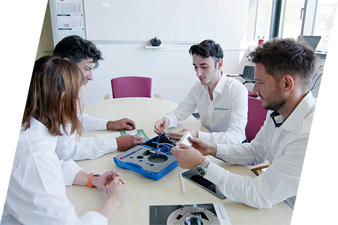
Your Partner for Piezo Solutions
- Customized solutions to fit your special requests
- Deep experience in the production and development of nano-positioning solutions
- Comprehensive consultation
- Worldwide partners, and fast support guaranteed
- Quick solution propositions
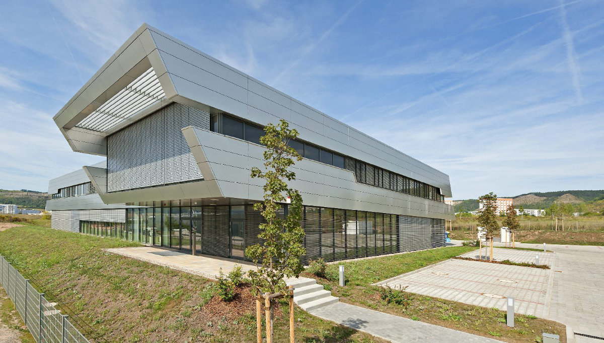
Established in 1991, piezosystem jena offers piezo micro-positioning, piezo nano-positioning and metrology solutions to the semiconductor, aerospace, microscopy and synchrotron community. We have an extensive knowledge and in-depth technical expertise in the application of piezo technology for nano-positioning tasks, and in the design of piezo flexure stages and development of piezomechanical systems.
The real strength of piezosystem jena comes from our commitment to complete customer satisfaction in the markets we serve. The partnerships we form with our clientele in applications such as super resolution microscopy, AFM, process control, semiconductor metrology and nano-positioning for synchrotron radiation are long-lasting and mutually beneficial. Our knowledge in piezo technology comes from our own research, and our daily interactions as consultants.
Outstanding Characteristics of Piezo Elements:
- Nearly unlimited resolution of movement (sub-nm)
- Extremely high maximum compressive forces (multiple kN)
- Movement without any mechanical play
- Very short response times
- No mechanical wear
- Suitable for vacuum applications
- Suitable for cryogenic temperatures
For a simple piezoelectric positioning system, or a complex design and consultation:
In Europe and Asia
Telefon: (+49) 3641 66 88-0
Fax: (+49) 3641 66 88 66
EMail: info(at)piezojena.com
In North America
Telephone: +1-508-634-6688
EMail: contact(at)psj-usa.com